- 您现在的位置:买卖IC网 > Sheet目录2003 > LTC1278-4IN#PBF (Linear Technology)IC A/DCONV SAMPLNG W/SHTDN 24DIP
13
LTC1278
DIGITAL INTERFACE
The A/D converter is designed to interface with micropro-
cessors as a memory mapped device. The CS and RD
control inputs are common to all peripheral memory interfac-
ing. A separate CONVST is used to initiate a conversion.
Internal Clock
The A/D converter has an internal clock that eliminates the
need of synchronization between the external clock and
the CS and RD signals found in other ADCs. The internal
clock is factory trimmed to achieve a typical conversion
time of 1.6
s. No external adjustments are required, and
with the typical acquisition time of 250ns, throughput
performance of 500ksps is assured.
Power Shutdown
The LTC1278 provides a shutdown feature that will save
power when the ADC is in inactive periods. To power down
the ADC, Pin 18 (SHDN) needs to be driven low. When in
power shutdown mode, the LTC1278 will not start a
conversion even though the CONVST goes low. All the
U
S
A
O
PPLICATI
WU
U
I FOR ATIO
Also, since any potential difference in grounds between
the signal source and ADC appears as an error voltage in
series with the input signal, attention should be paid to
reducing the ground circuit impedances as much as
possible.
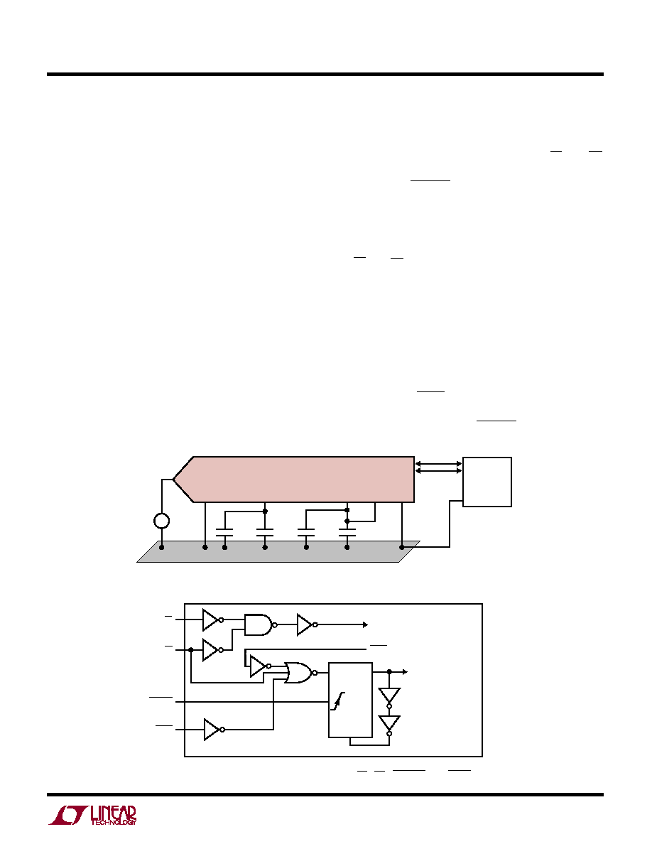
A single point analog ground separate from the logic
system ground should be established with an analog
ground plane at Pin 3 (AGND) or as close as possible to the
ADC. Pin 12 (DGND) and all other analog grounds should
be connected to this single analog ground point. No other
digital grounds should be connected to this analog ground
point. Low impedance analog and digital power supply
common returns are essential to low noise operation of
the ADC and the foil width for these tracks should be as
wide as possible. In applications where the ADC data
outputs and control signals are connected to a continu-
ously active microprocessor bus, it is possible to get
errors in conversion results. These errors are due to
feedthrough from the microprocessor to the successive
approximation comparator. The problem can be elimi-
nated by forcing the microprocessor into a WAIT state
during conversion or by using three-state buffers to iso-
late the ADC data bus.
Figure 11. Internal Logic for Control Inputs CS, RD, CONVST and SHDN
Figure 10. Power Supply Grounding Practice
LTC1278 F10
AIN
AGND
VREF
AVDD
DVDD
DGND
LTC1278
DIGITAL
SYSTEM
0.1
F
+
–
ANALOG GROUND PLANE
GROUND CONNECTION
TO DIGITAL CIRCUITRY
ANALOG
INPUT
CIRCUITRY
3
2
24
17
12
1
0.1
F
10
F
10
F
CONVERSION
START (RISING
EDGE TRIGGER)
LTC1278 F11
BUSY
FLIP
FLOP
CLEAR
Q
D
ACTIVE HIGH
ENABLE THREE-STATE OUTPUTS
DB11....DB0
CS
RD
CONVST
SHDN
发布紧急采购,3分钟左右您将得到回复。
相关PDF资料
LTC1279CG#TRPBF
IC A/DCONV SAMPLNG W/SHTDN24SSOP
LTC1282ACN#PBF
IC A/D CONV SAMPLING W/REF 24DIP
LTC1288IS8#TRPBF
IC A/D CONV SAMPLING 12BIT 8SOIC
LTC1298IS8#TRPBF
IC A/D CONV SAMPLING 12BIT 8SOIC
LTC1327CNW#PBF
IC TXRX EIA/TIA-562 3.3V 28-DIP
LTC1329ACS8-50#TRPBF
IC D/A CONV 8BIT MICROPWR 8-SOIC
LTC1337CNW#PBF
IC 3DVR/5RCVR 5V RS232 28-DIP
LTC1382IN#PBF
IC TXRX 5V RS232 W/SHTDWN 18-DIP
相关代理商/技术参数
LTC1278-4ISW
功能描述:IC A/DCONV SAMPLNG W/SHTDN24SOIC RoHS:否 类别:集成电路 (IC) >> 数据采集 - 模数转换器 系列:- 标准包装:1,000 系列:- 位数:12 采样率(每秒):300k 数据接口:并联 转换器数目:1 功率耗散(最大):75mW 电压电源:单电源 工作温度:0°C ~ 70°C 安装类型:表面贴装 封装/外壳:24-SOIC(0.295",7.50mm 宽) 供应商设备封装:24-SOIC 包装:带卷 (TR) 输入数目和类型:1 个单端,单极;1 个单端,双极
LTC1278-4ISW#PBF
功能描述:IC A/DCONV SAMPLNG W/SHTDN24SOIC RoHS:是 类别:集成电路 (IC) >> 数据采集 - 模数转换器 系列:- 标准包装:1,000 系列:- 位数:12 采样率(每秒):300k 数据接口:并联 转换器数目:1 功率耗散(最大):75mW 电压电源:单电源 工作温度:0°C ~ 70°C 安装类型:表面贴装 封装/外壳:24-SOIC(0.295",7.50mm 宽) 供应商设备封装:24-SOIC 包装:带卷 (TR) 输入数目和类型:1 个单端,单极;1 个单端,双极
LTC1278-4ISW#TR
功能描述:IC ADC 12BIT SAMPL SHTDWN 24SOIC RoHS:否 类别:集成电路 (IC) >> 数据采集 - 模数转换器 系列:- 标准包装:1,000 系列:- 位数:12 采样率(每秒):300k 数据接口:并联 转换器数目:1 功率耗散(最大):75mW 电压电源:单电源 工作温度:0°C ~ 70°C 安装类型:表面贴装 封装/外壳:24-SOIC(0.295",7.50mm 宽) 供应商设备封装:24-SOIC 包装:带卷 (TR) 输入数目和类型:1 个单端,单极;1 个单端,双极
LTC1278-4ISW#TRPBF
功能描述:IC A/DCONV SAMPLNG W/SHTDN24SOIC RoHS:是 类别:集成电路 (IC) >> 数据采集 - 模数转换器 系列:- 标准包装:1,000 系列:- 位数:12 采样率(每秒):300k 数据接口:并联 转换器数目:1 功率耗散(最大):75mW 电压电源:单电源 工作温度:0°C ~ 70°C 安装类型:表面贴装 封装/外壳:24-SOIC(0.295",7.50mm 宽) 供应商设备封装:24-SOIC 包装:带卷 (TR) 输入数目和类型:1 个单端,单极;1 个单端,双极
LTC1278-5CSW
功能描述:IC A/DCONV SAMPLNG W/SHTDN24SOIC RoHS:否 类别:集成电路 (IC) >> 数据采集 - 模数转换器 系列:- 其它有关文件:TSA1204 View All Specifications 标准包装:1 系列:- 位数:12 采样率(每秒):20M 数据接口:并联 转换器数目:2 功率耗散(最大):155mW 电压电源:模拟和数字 工作温度:-40°C ~ 85°C 安装类型:表面贴装 封装/外壳:48-TQFP 供应商设备封装:48-TQFP(7x7) 包装:Digi-Reel® 输入数目和类型:4 个单端,单极;2 个差分,单极 产品目录页面:1156 (CN2011-ZH PDF) 其它名称:497-5435-6
LTC1278-5CSW#PBF
功能描述:IC A/DCONV SAMPLNG W/SHTDN24SOIC RoHS:是 类别:集成电路 (IC) >> 数据采集 - 模数转换器 系列:- 其它有关文件:TSA1204 View All Specifications 标准包装:1 系列:- 位数:12 采样率(每秒):20M 数据接口:并联 转换器数目:2 功率耗散(最大):155mW 电压电源:模拟和数字 工作温度:-40°C ~ 85°C 安装类型:表面贴装 封装/外壳:48-TQFP 供应商设备封装:48-TQFP(7x7) 包装:Digi-Reel® 输入数目和类型:4 个单端,单极;2 个差分,单极 产品目录页面:1156 (CN2011-ZH PDF) 其它名称:497-5435-6
LTC1278-5CSW#TR
功能描述:IC ADC 12BIT SAMPL SHTDWN 24SOIC RoHS:否 类别:集成电路 (IC) >> 数据采集 - 模数转换器 系列:- 标准包装:1,000 系列:- 位数:12 采样率(每秒):300k 数据接口:并联 转换器数目:1 功率耗散(最大):75mW 电压电源:单电源 工作温度:0°C ~ 70°C 安装类型:表面贴装 封装/外壳:24-SOIC(0.295",7.50mm 宽) 供应商设备封装:24-SOIC 包装:带卷 (TR) 输入数目和类型:1 个单端,单极;1 个单端,双极
LTC1278-5CSW#TRPBF
功能描述:IC A/DCONV SAMPLNG W/SHTDN24SOIC RoHS:是 类别:集成电路 (IC) >> 数据采集 - 模数转换器 系列:- 标准包装:1,000 系列:- 位数:12 采样率(每秒):300k 数据接口:并联 转换器数目:1 功率耗散(最大):75mW 电压电源:单电源 工作温度:0°C ~ 70°C 安装类型:表面贴装 封装/外壳:24-SOIC(0.295",7.50mm 宽) 供应商设备封装:24-SOIC 包装:带卷 (TR) 输入数目和类型:1 个单端,单极;1 个单端,双极